Smart Bracelet Design Based on STM32 (Without LVGL) - Continuously Updated#
1. Pin Allocation#
| Device | Resource | Pin |
|---|---|---|
| OLED Display | Software IIC | SCL: PB8 SDA: PB9 |
| MPU6050 | Hardware IIC | I2C2: SCL: PB10 SDA: PB11 |
| MAX30102 | Software IIC | SCL: PC14 SDA: PC15 |
| DHT11 | Wire | PB6 |
| W25Q64 | Hardware SPI | SPI1: SS: PA4 SCK: PA5 MOSI: PA7 MISO: PA6 |
| ESP01 | Uart | Uart2: esp01(Tx): PA3 esp01(Rx): PA2 |
| MQ-2 | ADC/GPIO | ADC: PB0 GPIO: PB1 |
| Buzzer | GPIO | PB5 |
| Buttons (4) | GPIO | PA8 PA9 PA10 PA1 |
The modules and microcontroller resources used in this design draft are not fully applied in the actual design, but they are still retained in the diagram, and will be called upon when adding features later.
2. Design of Visual Operation Interface#
- Boot Screen
- Time
- Network Connection Information
- Menu Options
- Battery Display
- Menu Interface
- Weather Display
- Temperature and Humidity Information
- Pulse Information
- Personal Center
- Step Count Information
This project does not use the LVGL graphics library technology, but instead adopts a dot matrix drawing method for visual interface design, which tests the author's artistic skills. Due to the inefficiency of this method and its obvious shortcomings in other aspects, it is not recommended for use. Due to a busy schedule, the features have not been fully developed, and they will be gradually completed when time allows.
3. Cloud Design#
1. Cloud App Design#
For data uploading, we use the ESP8266 module + Dandelion Technology to upload the data obtained from STM32. We have created some data storage units on our Dandelion Technology App. With the Dandelion Technology App, we only need to click the compile button in the upper right corner to freely add various devices we want.
2. Data Upload and Communication#
2.1 Data Upload#
For data uploading, we use the ESP8266 module combined with the Arduino framework. Dandelion Technology has designed a software framework on Arduino that supports interaction between the ESP series and the cloud. We just need to call the library functions to achieve the desired functionality.
(1) Development Environment Preparation#
-
First, we need to obtain the ESP8266 development board support package; there are many tutorials online. We can install the ESP8266 support package through this blog. (13 messages) Setting up the Esp8266 Development Environment with Arduino (Two Methods) arduino esp8266℡Four-leaf Clover~'s Blog-CSDN Blog
-
If we have already installed the ESP8266 support package, we need to install the official Blinker library,
- First, click "Project," find the "Load Library" option, click it, find "Manage Libraries," and click in.
- In the input box of this dialog, enter Blinker, then select the version; my version is 0.3.9, and then click install. Wait a moment to complete the installation. Since this is using an external network, the download speed may be slow, so please be patient.
(2) Program Design#
- First, we need to include the header file.
#define BLINKER_PRINT Serial
#define BLINKER_WIFI

#include <Blinker.h>
-
Connect to Wi-Fi and to Dandelion Technology
(1) First, define three character arrays and add your information.
// Connection information
char auth[] = "your_key";
char ssid[] = "your_wifi_name";
char pswd[] = "your_wifi_password";
(2) In void setup(), call the following function to complete the connection to Wi-Fi and the Dandelion Technology server.
Blinker.begin(auth, ssid, pswd);
(3) To execute data uploading, we first need to create components, then create data storage objects, and finally execute data printing in the heartbeat packet or other functions. This way, the obtained data will be displayed under the components we created, and we can also send data to ESP01 through Dandelion Technology. Here we implemented a switch light function.
Note: The string passed when creating the component object should be exactly the same as the component object name created on Dandelion Technology; otherwise, we cannot achieve the desired functionality.
// Create component objects
BlinkerButton Button1("btn-1");
BlinkerNumber Tem("tem");
BlinkerNumber Hum("hum");
BlinkerNumber Smoke("smoke");
BlinkerNumber Maibo("maibo");
BlinkerNumber Bushu("bushu");

// The function will be executed when the button is pressed
void button1_callback(const String & state) {
    BLINKER_LOG("get button state: ", state);
    digitalWrite(Esp01_Led, !digitalRead(Esp01_Led));
}

// Cloud storage temperature and humidity data function
void dataStorage()
{
    Blinker.dataStorage("temp_chart", (float)tem); // Store temperature
    Blinker.dataStorage("hum_chart", (float)tem);  // Store humidity
    Blinker.dataStorage("smoke_chart", (float)smoke); // Store smoke
    Blinker.dataStorage("maibo_chart", (int)maibo); // Store maibo
    Blinker.dataStorage("bushu_chart", (uint32_t)bushu); // Store bushu
}

// Heartbeat packet
void heartbeat(){
    Hum.print((float)hum);
    Tem.print((float)tem);
    Smoke.print((float)smoke);
    Maibo.print((int)maibo);
    Bushu.print((uint32_t)bushu);
}

void setup() {
    // Initialize serial port
    Serial.begin(115200);

    #if defined(BLINKER_PRINT)
        BLINKER_DEBUG.stream(BLINKER_PRINT);
    #endif

    // Initialize IO with LED
    pinMode(Esp01_Led, OUTPUT);
    digitalWrite(Esp01_Led, HIGH);
    // Initialize Blinker
    Blinker.begin(auth, ssid, pswd);
    Button1.attach(button1_callback);
    Blinker.attachHeartbeat(heartbeat);
}
2.2 Data Communication#
In the entire smart bracelet design system, the ESP01 we use is just an auxiliary module; the real module executing data acquisition and interaction design is still our STM32. ESP01 supports serial communication, so we use serial communication to interact with STM32. For this need, we have designed a set of data communication rules.
(1) ESP01 Communication Design#
- Our requirements are roughly divided into two parts: sending and uploading. After comprehensive consideration, we decided to adopt the interaction communication method between ESP01 and STM32, using CRC checksums and cumulative checks for data verification. Based on this method, we defined many data commands on the ESP01 side. For example, when STM32 sends 0xFF to ESP01, ESP01 will return the obtained time data (3 bytes for hours, minutes, seconds + 1 checksum byte).
void CmdMode::Run(ModeManager *manager){
	cmd = 0x00;
    if(Serial.available()){
        cmd = Serial.read();
    }
	// Get time data command, ESP01 will send hours, minutes, seconds, and checksum to STM32
    if(cmd == 0xff){
        Serial.write(hour1); // Hour
        Serial.write(minute1); // Minute
        Serial.write(sec1); // Second
        Serial.write(hour1 + minute1 + sec1); // Checksum
    }
	// Get temperature data command, switch to temperature reception mode
    else if(cmd == 0xfe){
        Mode *tem_pin;
        tem_pin = manager->rd;
        manager->setRd(new TemdataMode());
        delete tem_pin;
    }
	// Get smoke data command, switch to smoke reception mode
    else if(cmd == 0xfd){
        Mode *tem_pin;
        tem_pin = manager->rd;
        manager->setRd(new SmokedataMode());
        delete tem_pin;
    }
	// Get temperature and humidity mode, switch to temperature and humidity reception mode
    else if(cmd == 0xfc){
        Mode *tem_pin;
        tem_pin = manager->rd;
        manager->setRd(new MaibodataMode());
        delete tem_pin;
    // Get step count mode, switch to step count reception mode
    else if(cmd == 0xfb){
        Mode *tem_pin;
        tem_pin = manager->rd;
        manager->setRd(new BushudataMode());
        delete tem_pin;
    }
}
- Due to the numerous data commands between the two, it can easily cause unnecessary confusion during development. In the program design process, we adopted the State Pattern from the 23 Object-Oriented Design Patterns to achieve decoupling of different commands. Although we need to continuously create and destroy objects during state switching, this pattern greatly improves our program's maintainability and saves a lot of conditional checks.
(2) STM32 Communication Design#
Based on the communication program designed on the ESP01 side, we only need to use commands to receive data uploads on the STM32 side, which is simple and convenient. For example, when we need to upload temperature and humidity information, we only need to send the command 0xFE on the STM32 side, and then we send the data we need to ESP01 (two data bits (temperature, humidity), checksum (which is the sum of the two)).
	Serial_SendByte(0xfe);
	Serial_SendByte(tem);
	Serial_SendByte(hum);
	Serial_SendByte(tem + hum);
4. Function Design#
4.1 DHT11 Temperature and Humidity Information Acquisition#
DHT11 is a digital temperature and humidity sensor module, and its conversion results can be directly output through a single bus digital signal. It is a commonly used environmental temperature and humidity measurement module. This module uses a high-quality temperature and humidity sensor, featuring high precision, long lifespan, and good stability. It has characteristics such as fast response and stable output, making it easy to interface with most microcontrollers and communicate via a single bus. In addition to measuring the environmental temperature and humidity values, this module can also set upper and lower limits. When the environmental temperature and humidity exceed the set range, it will generate an alarm signal. The DHT11 module is widely used in home automation, the Internet of Things, and environmental monitoring.

(1) DHT11 uses the Wire single bus communication protocol, which is a half-duplex, asynchronous communication method. As the master, the STM32 microcontroller must first send a command to DHT11 to receive data before we can proceed with data reception. Therefore, in the design of the driver program, we need to set the STM32 port to output mode in advance. Here we set it to push-pull output and then set the port level to high.
/**
  * @brief  DHT11 initialization
  * @param  None (During initialization, we set the pin mode to push-pull output)
  * @retval None
  */
void DHT11_Init(void)
{
	RCC_APB2PeriphClockCmd(RCC_APB2Periph_GPIOB, ENABLE);

    GPIO_InitTypeDef GPIO_InitStruct;

    GPIO_InitStruct.GPIO_Pin = DHT11_PIN;
    GPIO_InitStruct.GPIO_Mode = GPIO_Mode_Out_PP;
    GPIO_InitStruct.GPIO_Speed = GPIO_Speed_50MHz;
    GPIO_Init(DHT11_GPIO, &GPIO_InitStruct);

    GPIO_SetBits(DHT11_GPIO, DHT11_PIN);
}
(2) The reading data cycle of the Wire single bus is at least 60us, and there must be at least 1us recovery time between two independent read time slots. Each read time slot is initiated by the master, which must pull the bus low for at least 1us. After the master initiates the read time slot, the single bus device will start sending 0 or 1 on the bus.
If the slave sends 1, it keeps the bus high; if it sends 0, it pulls the bus low. When sending 0, the slave releases the bus after the time slot ends, allowing the pull-up resistor to pull the bus back to the idle high state. The data sent by the slave remains valid for 15us after the start time slot, so the master must release the bus during the read time slot and sample the bus state within 15us after the start of the time slot.
(3) Therefore, in the program design, we wait for 30us to delay until the master can read the byte. The general logic is: wait for the low level end of the read command sent by the master -> wait 30us -> read level -> wait for level end.
/**
  * @brief  DHT11 read byte
  * @param  None (The judgment logic is: when the bus is pulled low, wait for 30us; if it is high afterward, it is judged as 1; otherwise, it is 0)
  * @retval None
  */
uint8_t DHT11_Read_Byte(void)
{
    uint8_t i, data = 0;

    for (i = 0; i < 8; i++)
    {
        while (!GPIO_ReadInputDataBit(DHT11_GPIO, DHT11_PIN)); // Wait for low level end
        Delay_us(30);
        if (GPIO_ReadInputDataBit(DHT11_GPIO, DHT11_PIN)) // High level starts
            data |= (1 << (7 - i));
        while (GPIO_ReadInputDataBit(DHT11_GPIO, DHT11_PIN)); // Wait for high level end
    }

    return data;
}
(4) To send the level reading command to DHT11, we need to pull the bus low for at least 480us to enter RX receive mode, and then pull the bus high. In the code, we reconfigure the IO port mode to floating input mode and then proceed to receive data.

/**
  * @brief  DHT11 data
  * @param  None
  * @retval None
  */
void DHT11_Read_Data(uint8_t* temp, uint8_t* humi)
{
    uint8_t data[5], i;

    GPIO_InitTypeDef GPIO_InitStruct;

    GPIO_InitStruct.GPIO_Pin = DHT11_PIN;
    GPIO_InitStruct.GPIO_Mode = GPIO_Mode_Out_PP;
    GPIO_InitStruct.GPIO_Speed = GPIO_Speed_50MHz;
    GPIO_Init(DHT11_GPIO, &GPIO_InitStruct);

	// Pull low for at least 480us to enter RX receive mode
    GPIO_ResetBits(DHT11_GPIO, DHT11_PIN);
    Delay_us(600);
    GPIO_SetBits(DHT11_GPIO, DHT11_PIN);
    Delay_us(30);
	// When reading data, we need to switch the GPIO port
    GPIO_InitStruct.GPIO_Mode = GPIO_Mode_IN_FLOATING;
    GPIO_Init(DHT11_GPIO, &GPIO_InitStruct);

    if (!GPIO_ReadInputDataBit(DHT11_GPIO, DHT11_PIN))
    {
        while (!GPIO_ReadInputDataBit(DHT11_GPIO, DHT11_PIN)); // Wait for low level end
        while (GPIO_ReadInputDataBit(DHT11_GPIO, DHT11_PIN)); // Wait for high level start
        for (i = 0; i < 5; i++)
            data[i] = DHT11_Read_Byte();
		// Checksum is the sum of the first 4 bytes of data
        if (data[4] == (data[0] + data[1] + data[2] + data[3]))
        {
            *humi = data[0];
            *temp = data[2];
        }
    }
}
4.2 Max30102 Pulse Detection#
Max30102 is a highly integrated precision heart rate sensor module that uses proprietary optical sensing technology and advanced digital signal processing devices to quickly and accurately measure physiological indicators such as heart rate and pulse oxygen saturation (SpO2). This module has a high-brightness LED light source and a photodetector that can quickly collect the reflected light signal from the skin area of the subject and convert it into an electrical signal output. Max30102 supports different sampling rates and resolution settings, and implements on-chip data filtering, calibration, and adjustment functions through a built-in DC adjustable gain amplifier and 8-bit ADC. This module also provides an I2C interface for communication, making it easy to interface with most microcontrollers and allowing direct data acquisition, threshold setting, LED control, and other operations. Currently, the Max30102 module is mainly used in health monitoring, medical devices, and sports training.

(1) I2C (Inter-Integrated Circuit) is a serial communication bus protocol commonly used for communication between integrated circuits. It was introduced by Philips (now NXP) and is often used in various embedded systems. The I2C protocol uses a two-wire system, one called SDA (Serial Data) and the other called SCL (Serial Clock). The SDA line is used for data transmission, while the SCL line is used for clock synchronization, allowing for bidirectional communication between devices. Based on its nature, we know it is a half-duplex, synchronous communication protocol.
(2) Based on the MAX30102 data manual, we have collected some data commands related to this chip, which we list here using macro definitions.
#define max30102_WR_address 0xAE

#define I2C_WRITE_ADDR 0xAE
#define I2C_READ_ADDR 0xAF

// Register addresses
#define REG_INTR_STATUS_1 0x00
#define REG_INTR_STATUS_2 0x01
#define REG_INTR_ENABLE_1 0x02
#define REG_INTR_ENABLE_2 0x03
#define REG_FIFO_WR_PTR 0x04
#define REG_OVF_COUNTER 0x05
#define REG_FIFO_RD_PTR 0x06
#define REG_FIFO_DATA 0x07
#define REG_FIFO_CONFIG 0x08
#define REG_MODE_CONFIG 0x09
#define REG_SPO2_CONFIG 0x0A
#define REG_LED1_PA 0x0C
#define REG_LED2_PA 0x0D
#define REG_PILOT_PA 0x10
#define REG_MULTI_LED_CTRL1 0x11
#define REG_MULTI_LED_CTRL2 0x12
#define REG_TEMP_INTR 0x1F
#define REG_TEMP_FRAC 0x20
#define REG_TEMP_CONFIG 0x21
#define REG_PROX_INT_THRESH 0x30
#define REG_REV_ID 0xFE
#define REG_PART_ID 0xFF
(3) Based on the data command set, we call the data line (SDA) to send commands and encapsulate them in function form.
void max30102_init(void);
void max30102_reset(void);
u8 max30102_Bus_Write(u8 Register_Address, u8 Word_Data);
u8 max30102_Bus_Read(u8 Register_Address);
void max30102_FIFO_ReadWords(u8 Register_Address, u16 Word_Data[][2], u8 count);
void max30102_FIFO_ReadBytes(u8 Register_Address, u8* Data);

void maxim_max30102_write_reg(uint8_t uch_addr, uint8_t uch_data);
void maxim_max30102_read_reg(uint8_t uch_addr, uint8_t *puch_data);
void maxim_max30102_read_fifo(uint32_t *pun_red_led, uint32_t *pun_ir_led);
4.3 Time and Weather Acquisition#
(1) Time Acquisition#
For time acquisition, the Blinker official library has its encapsulated API functions. We just need to call them to achieve time acquisition, and then use serial communication to package the time data and send it to STM32, finally displaying it on the visual interface.
   	// Time data acquisition
	hour1 = Blinker.hour();
    minute1 = Blinker.minute();
    sec1 = Blinker.second();
	// Time data return
    if(cmd == 0xff){
      Serial.write(hour1);
      Serial.write(minute1);
      Serial.write(sec1);
      Serial.write(hour1 + minute1 + sec1);
    }
(2) Weather Acquisition#
4.4 Step Count Calculation and Acquisition#
4.5 Personal Center Design#
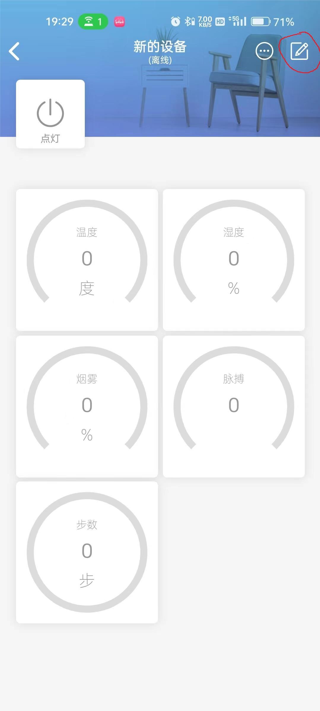
The personal center actually provides real-time monitoring of the wearer's health information, focusing on two aspects: "Pulse and Blood Oxygen Saturation Monitoring" and "Smoking Monitoring." It utilizes the smoke module and Max30102 module to monitor smoke, pulse, and blood oxygen concentration at regular intervals, using the data as a reference to determine whether the wearer is smoking and whether their heart rate and blood oxygen levels are normal. The data is uploaded to the cloud in real-time to monitor the wearer's health status, ensuring the wearer's physical well-being.
(1) The smoke module we use is MQ2, which has four pins: VCC, GND, AO, and DO, where AO and DO correspond to the digital output and analog output ports, respectively. We use the AO analog output port.

(2) When reading data, we need to configure the STM32 port (select a port that supports ADC functionality) to analog input mode. The built-in ADC module of STM32 will automatically complete the ADC conversion. Finally, we read the analog value. To convert the data into a percentage format, we normalize the current value to map it between 0 and 1, multiply by 100, and finally obtain the desired percentage format.
#include "Smoke.h"                  // Device header

/**
  * @brief  ADC initialization
  * @param  None
  * @retval None
  */
void Smoke_Init(void)
{
	// Define related structures for parameter configuration
	GPIO_InitTypeDef GPIO_InitStructure;
	ADC_InitTypeDef ADC_InitStructure;
	// Enable ADC and GPIOA bus
	RCC_APB2PeriphClockCmd(RCC_APB2Periph_ADC1, ENABLE);
	RCC_APB2PeriphClockCmd(RCC_APB2Periph_GPIOB, ENABLE);
	// Configure clock division
	RCC_ADCCLKConfig(RCC_PCLK2_Div6);
	// Configure GPIO mode. Mode is ADC input
	GPIO_InitStructure.GPIO_Mode = GPIO_Mode_AIN;
	GPIO_InitStructure.GPIO_Pin = GPIO_Pin_0;
	GPIO_InitStructure.GPIO_Speed = GPIO_Speed_50MHz;
	GPIO_Init(GPIOB, &GPIO_InitStructure);
	//
	ADC_RegularChannelConfig(ADC1, ADC_Channel_8, 1, ADC_SampleTime_55Cycles5);
	// Configure ADC related parameters
	ADC_InitStructure.ADC_Mode = ADC_Mode_Independent;	// Set to independent mode
	ADC_InitStructure.ADC_DataAlign = ADC_DataAlign_Right;	// Specify data as right-aligned
	// Configure ADC related parameters
	ADC_InitStructure.ADC_ExternalTrigConv = ADC_ExternalTrigConv_None;	// No external trigger
	ADC_InitStructure.ADC_ContinuousConvMode = DISABLE;	// Disable continuous conversion mode
	ADC_InitStructure.ADC_ScanConvMode = DISABLE; // Disable scan mode
	ADC_InitStructure.ADC_NbrOfChannel = 1;	// Specify ADC channel
	ADC_Init(ADC1, &ADC_InitStructure);
	// Start ADC1
	ADC_Cmd(ADC1, ENABLE);

	ADC_ResetCalibration(ADC1);		// Reset calibration register
	while(ADC_GetResetCalibrationStatus(ADC1) == SET);	// Wait for calibration to complete
	ADC_StartCalibration(ADC1);	// Start calibration function
	while(ADC_GetCalibrationStatus(ADC1) == SET);	// Wait for start to complete
}

/**
  * @brief  Get the quantized data after ADC conversion
  * @param  None
  * @retval The converted ADC value
  */
uint16_t Smoke_GetValue(void)
{
	ADC_SoftwareStartConvCmd(ADC1, ENABLE);	// Software start ADC1 clock
	while(ADC_GetFlagStatus(ADC1, ADC_FLAG_EOC) == RESET);	// Wait for ADC conversion to complete
	return ADC_GetConversionValue(ADC1);	// Return the converted value
}
(3) To monitor the wearer's health status in real-time and avoid blocking the main program operation due to excessive monitoring frequency, we set the sampling interval for pulse, blood oxygen concentration, and smoke acquisition tasks to 1 minute. We can view specific data on the Dandelion Technology APP or in the personal center on the bracelet. If any of these three sets of data falls below normal values, the bracelet will issue an alarm and send the data to the cloud to alert passersby and family members.